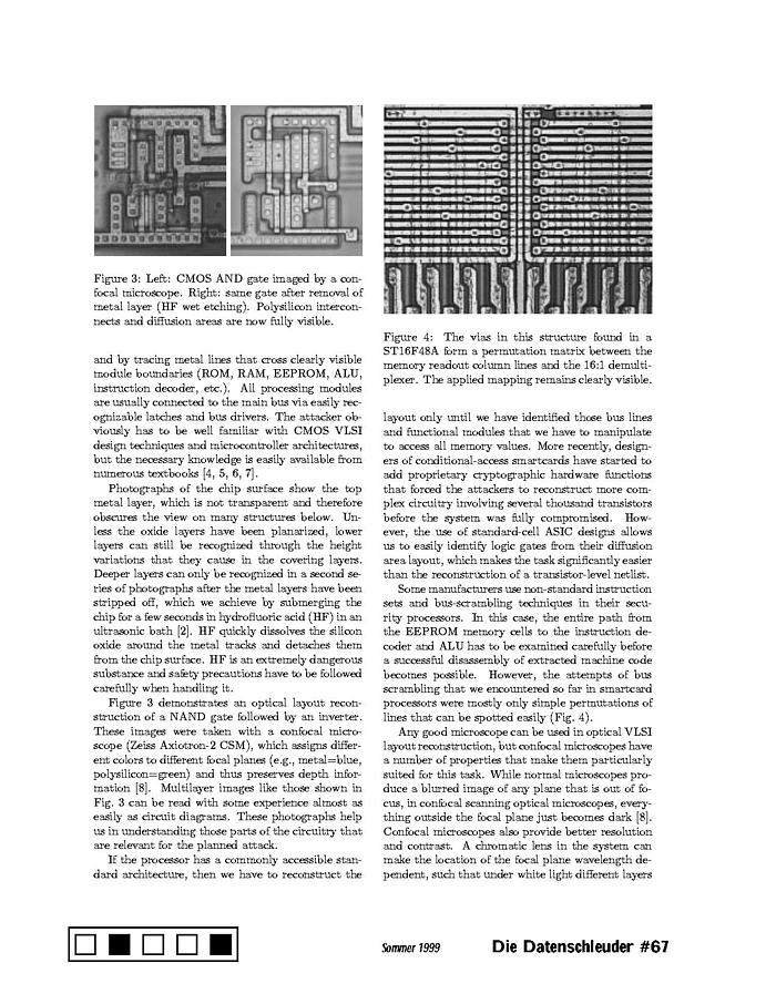
Labels:text | newspaper | screenshot | publication | black and white | paper | printing | font OCR: Figure 3: Left: CMOS AND gate imaged by a con- focal tmicroscope, Right: same gate after removal of metal layer (HF wet etching). Polysilicon intercon- bects and diffusion areas are now fully visible. Figure 4: The vias in this structure found in a and by tracing metal lines that cross clearly visible ST16F48A form a permutation matrix between the tnodule boundaries (ROM, RAM, EEPROM, ALU, memory readout column lines and the 16:1 demulti- instruction decoder, etc.). All processing modules plexer. The applied mapping remains clearly visible. are usually connected to the main bus via easily rec- oghizable latches and bus drivers. The attacker ob- viously has to be well familiar with CMOS VLSI layout only until we have identified those bus lines design techniques and microcontroller architect ...